Fraunhofer develops PFAS-free polymer membrane for semiconductors
Iranpolymer/Baspar The semiconductor industry is at an all-time high. Nvidia, a US-based semiconductor designer, became the world’s most valuable company on June 19, surpassing Microsoft and hitting a market cap on $3.34 trillion.
A threat looms, however – and polymers might be the solution.
Semiconductor manufacturing currently requires the use of per- and polyfluoroalkyl substances (PFAS), due to their stability and resistance to water and grease.
As PFAS bans threaten to impact this billion-dollar industry, stakeholders have turned to find viable, safe, long-term alternatives to these chemicals.
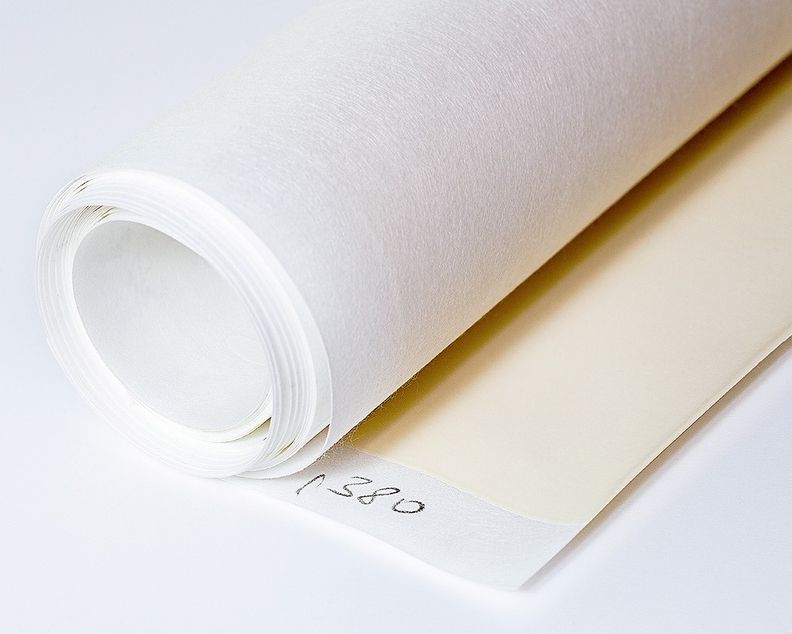
The Fraunhofer Institute for Applied Polymer Research (IAP) is contributing to these efforts by finding an alternative to PFAS membranes used during the semiconductor manufacturing process.
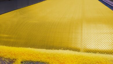
The German institute has developed a PFAS-free polymer membrane for use in filters or in the etching and cleaning processes.
The polyacrylonitrile (PAN) membrane is based on conventional, specifically stabilised polymers, and offers high chemical and mechanical stability. With a pore diameter of around 7 nanometres, the membrane can separate out ultra-small impurities from production and filtering whilst allowing in the fluids required for the process, such as acids and solvents.
“Chip manufacturing involves numerous process steps such as cutting, cleaning, and planarisation to apply the structures to the wafer,” explained Dr. Murat Tutus, engineer at Fraunhofer IAP. “All of these operations produce particulate contaminants that must be separated out in each process, otherwise they would interfere with the creation of nanometersised structures. We were able to use another component patented by us to chemically modify the polymer and stabilise it also for harsh environments,” he added.
Polyacrylonitrile is a synthetic, semi-crystalline organic polymer resin often used a precursors for carbon fibre and fibre to make knitted clothing like socks and sweaters, as well as outdoor products like tents.
The membrane is produced using REACH-compliant solvents and low temperatures, making it an overall sustainable process, the IAP said. It is fabricated using a non-solvent induced phase separation process, which allows researchers to customise the pressure stability of the membrane.
One of the challenges required the team to find the ideal pore distribution whilst maintaining a very small pore size, which lowers permeability.
“The degree of permeability is defined by the number of pores on the surface. The smaller the pores, the lower the permeability. To increase permeability, we therefore had to increase the number of pores in a second step while keeping the pore size constant,” explains Tutus.
The membrane can be customised to meet specific needs, which makes it easy to integrate the new process into existing systems to manufacture the next generation of chips, the IAP said in a statement.
sustainableplastics